HDI PCB is among the fastest growing PCBs on the market because it meets complex design needs. This kind of high density interconnect printed circuit board allows designers to place more components in a smaller area. Having a higher circuitry density than conventional PCBs, it's able to incorporate finer lines and spaces, smaller vias & capture pads, and higher connection pad densities. It contains blind/buried vias and is often with 6 mil microvias.
HDI custom PCB is widely used to reduce the weight and overall dimensions of products, as well as enhancing the electrical performance of the device. It's regularly found in mobile phones, touch-screen devices, and 4G network communications.
China Dragon offers HDI custom PCB fabrication with microvias down to 4 mil; laser drilling is required.
HDI Structures
| HDI Structures | Type of micorovias | Mass production | Middle/small batch | Prototype | Apply to |
| 1+N+1 | Blind vias | Yes | Yes | Yes | 4 layers+ |
| 2+N+2 | Blind/Buried staggered vias | Yes | Yes | Yes | 6 layers+ |
| 2+N+2 | Blind/Buried stacked vias | Yes | Yes | Yes | 6 layers+ |
| 3+N+3 | Blind/Buried staggered vias | / | Yes | Yes | 8 layers+ |
| 3+N+3 | Blind/Buried stacked vias | / | / | Yes | 8 layers+ |
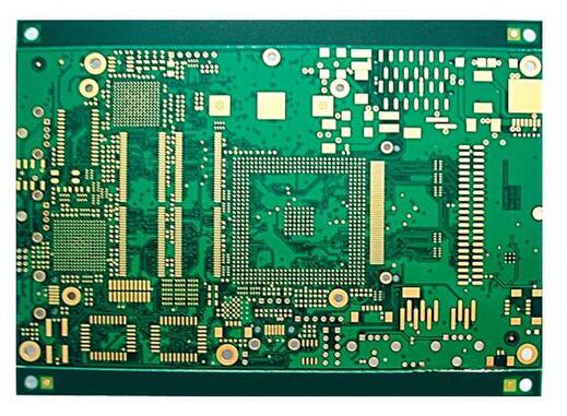
Sample HDI PCB fabricated by JingHon

If you have a requirement for copper weight options which is not listed on the online quotation form, feel free to send your design file together with a quote request to sales@pcbamfrs.com, quotation for your HDI custom PCB project will be provided very quickly.